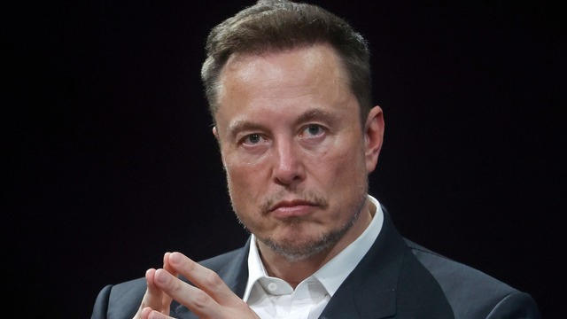
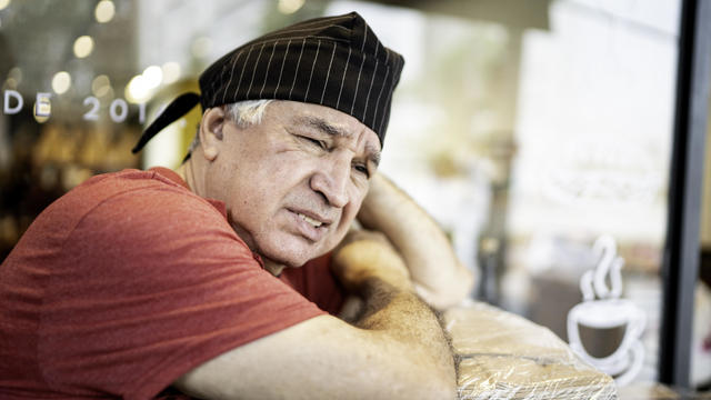
As EV sales slump, Tesla shares relinquish a year's worth of gains
Tesla's stock price has tumbled 39% this year amid concerns about the electric vehicle maker's slowing growth.
Watch CBS News
Tesla's stock price has tumbled 39% this year amid concerns about the electric vehicle maker's slowing growth.

House Speaker Mike Johnson is including the TikTok divest-or-ban bill in an aid package for Ukraine and Israel.

The U.S. is reaching "peak 65," marking the largest retirement wave in American history. But the financial outlook for many is grim.

Italy joins a long list of countries offering foreigners the opportunity to relocate, laptops in tow.
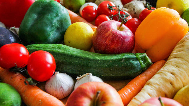
Organic option is best when buying certain produce, especially blueberries, nonprofit group says in analysis of chemical residues.
Nine workers arrested after demonstrations at the tech giant's offices n New York and California.

Health officials are warning consumers not to consume the Infinite Herbs basil sold at Trader Joe's after 12 people were sickened.
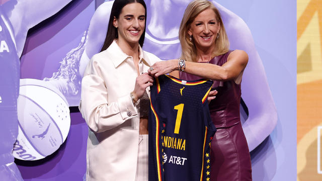
The No. 1 pick in this year's WNBA draft is "going to raise all boats" for players in the league, one expert said.
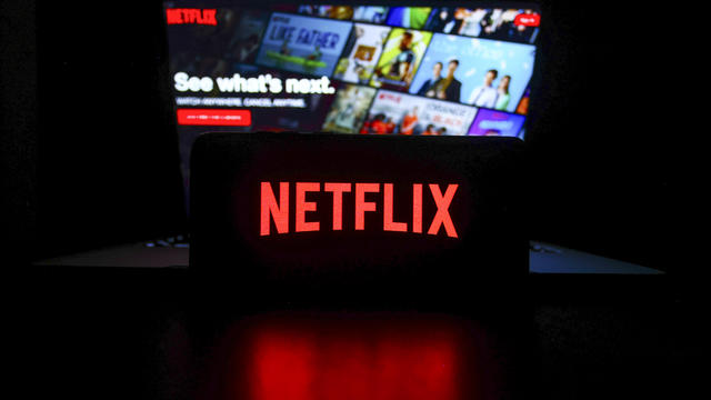
"Ultimately we think this is a better approach that reflects the evolution of the business," Netflix Co-CEO Greg Peters said on an earnings call.

Both types of gold assets could be a smart bet in today's economic environment. Here's why.

Considering tapping into your home equity? Here's how much you'd save when compared to your other options.

Are you shopping for long-term care insurance in your 70s? Make these three smart moves.
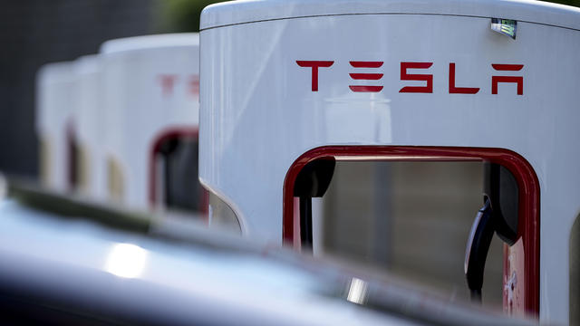
Tesla accounted for 80% of electric vehicle sales in the U.S. in 2020, but that figure fell to 55% last year.
The generative artificial intelligence boom has led to the emergence of romantic companion bots.

Apple said it will stop selling the devices later this month in order to comply with a U.S. import ban.
Alex Jones, the conspiracy theorist known for his fake news site InfoWars and his false denial of the Sandy Hook massacre, was permanently banned from Twitter in 2018.
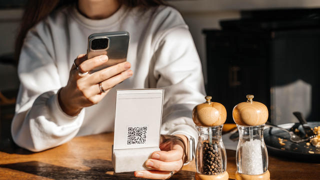
More than 90 million consumers will scan a QR code this year. But the technology can also facilitate identity theft.
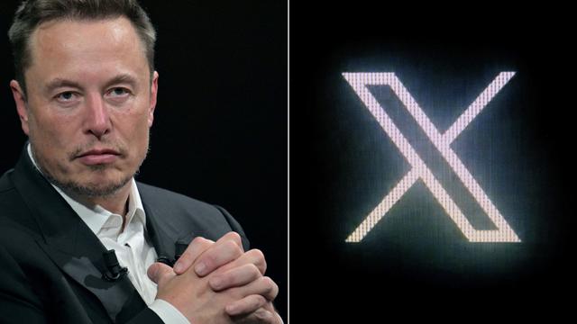
The billionaire owner of X took a defensive tone, saying that "the whole world will know that those advertisers killed the company."
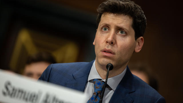
OpenAI co-founder Sam Altman says he's looking forward to returning to the company, with the support of Microsoft's CEO, to build the 2 companies' "strong partnership."
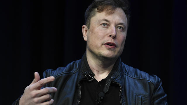
Musk, who is under fire for supporting an antisemitic post, said the money will be donated to hospitals in Israel and to the Red Cross in Gaza.
Altman landed at Microsoft, the biggest investor in OpenAI, as former Twitch leader Emmett Shear was named OpenAI's new chief executive.

Israel launched at least one missile strike at Iran early Friday morning, U.S. officials confirmed to CBS News, in apparent retaliation for last weekend's drone and missile attack.
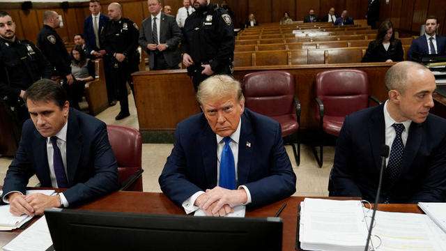
Twelve people have been selected to serve as jurors in former President Donald Trump's criminal trial in New York, filling out the panel on the third day of proceedings.
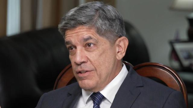
Cuba's deputy foreign minister tells CBS News that his country is willing to accommodate more than one deportation flight per month.
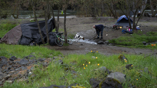
The Supreme Court will consider Monday whether bans on public camping constitute "cruel and unusual punishment" barred by the Eighth Amendment.
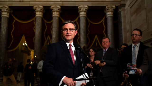
House Rules allow a single member to force a vote on ousting the speaker. Conservatives want to keep it that way.
His comments come as a deadlocked Congress continues to stall on Ukraine aid.
Rep. Ilhan Omar's daughter says she was one of three students suspended from Barnard College following a pro-Palestinian protest at Columbia University on Thursday.
Dubai is known for using planes to help prompt precipitation over the region. But experts say it did not play a role in this week's historic downpour.
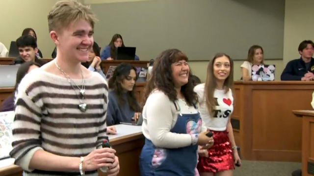
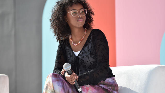
Taylor Swift's successes and failures, including the battle to regain control of her master recordings, are part of the syllabus at the University of California, Berkeley.
The U.S. is reaching "peak 65," marking the largest retirement wave in American history. But the financial outlook for many is grim.

Americans are underprepared for retirement, with the average account holding just $88,400 in savings.
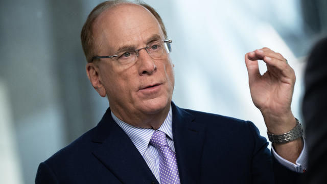
BlackRock CEO Larry Fink said that longer life expectancies are "putting the U.S. retirement system under immense strain."

About 1 in 8 workers think they'll retire by age 61. But the reality of saving for decades of expenses is daunting.
America's retirement system has left behind 90% of workers. "We see big gaps with the rich and the poor in terms of who gets to retire," one expert said.
"Ultimately we think this is a better approach that reflects the evolution of the business," Netflix Co-CEO Greg Peters said on an earnings call.
Taylor Swift's successes and failures, including the battle to regain control of her master recordings, are part of the syllabus at the University of California, Berkeley.
Prosecutors allege one of the suspects, Tifany Adams, provided a statement to law enforcement "indicating her responsibility" in the killings.
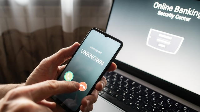
"Their job is to protect our investments," said one man whose bank account was drained of $15,000. "Otherwise, what's the point of putting it with a bank?"
Online furniture and home furnishings seller says it is opening a brick-and-mortar location in May.
"Ultimately we think this is a better approach that reflects the evolution of the business," Netflix Co-CEO Greg Peters said on an earnings call.
"Their job is to protect our investments," said one man whose bank account was drained of $15,000. "Otherwise, what's the point of putting it with a bank?"
Online furniture and home furnishings seller says it is opening a brick-and-mortar location in May.
Tesla's stock price has tumbled 39% this year amid concerns about the electric vehicle maker's slowing growth.
Italy joins a long list of countries offering foreigners the opportunity to relocate, laptops in tow.
His comments come as a deadlocked Congress continues to stall on Ukraine aid.
Israel launched at least one missile strike at Iran early Friday morning, U.S. officials confirmed to CBS News, in apparent retaliation for last weekend's drone and missile attack.
Rep. Ilhan Omar's daughter says she was one of three students suspended from Barnard College following a pro-Palestinian protest at Columbia University on Thursday.
House Rules allow a single member to force a vote on ousting the speaker. Conservatives want to keep it that way.
Cuba's deputy foreign minister tells CBS News that his country is willing to accommodate more than one deportation flight per month.
Health officials are warning consumers not to consume the Infinite Herbs basil sold at Trader Joe's after 12 people were sickened.
A landmark review for Britain's National Health Service found young people have been let down by "remarkably weak" evidence backing medical interventions in gender care.
Organic option is best when buying certain produce, especially blueberries, nonprofit group says in analysis of chemical residues.
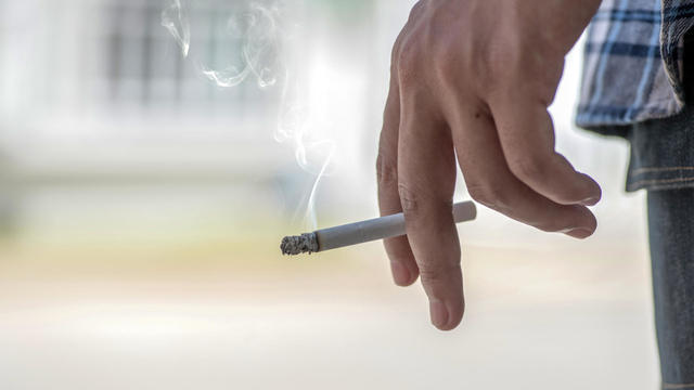
British lawmakers have backed legislation that would see the legal age to buy tobacco increase by one year every year until it's eventually banned.

A new generation of deodorant products promise whole-body odor protection. Should you try one? Dermatologists share what to know.
His comments come as a deadlocked Congress continues to stall on Ukraine aid.
Israel launched at least one missile strike at Iran early Friday morning, U.S. officials confirmed to CBS News, in apparent retaliation for last weekend's drone and missile attack.
Cuba's deputy foreign minister tells CBS News that his country is willing to accommodate more than one deportation flight per month.

Two officers survived the plane crash in Elgeyo Marakwet county, about 250 miles northwest of Nairobi, Kenya.

Elections are set to kick off in India, the world's biggest democracy, but there's concern that democratic values are being eroded.
"Ultimately we think this is a better approach that reflects the evolution of the business," Netflix Co-CEO Greg Peters said on an earnings call.
Taylor Swift's successes and failures, including the battle to regain control of her master recordings, are part of the syllabus at the University of California, Berkeley.
Taylor Swift's successes and failures, including the battle to regain control of her master recordings, are part of the syllabus at the University of California, Berkeley. Jo Ling Kent has more.

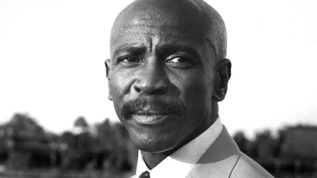
Dickey Betts, a guitarist and founding member of the Allman Brothers Band, has died at the age of 80 following a battle with cancer. Betts wrote some of the bands biggest hits, including "Ramblin' Man."
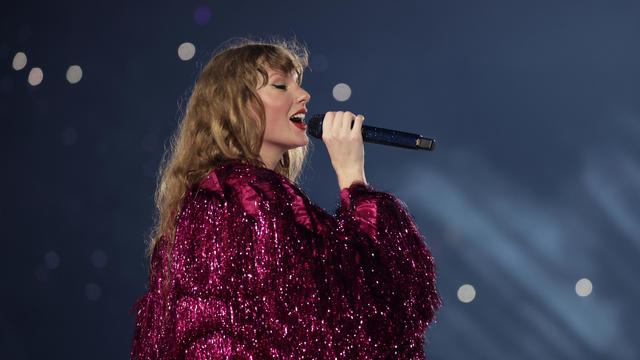
Taylor Swift took to social media hours ahead of the expected release of her new album "The Tortured Poets Department."
A bipartisan group of lawmakers has introduced a bill supporting the development of nuclear fusion power. Hank Jenkins-Smith, professor of public policy at the University of Oklahoma, joins CBS News to discuss.
Sen. Maria Cantwell is backing an amended bill that could lead to a ban of TikTok in the U.S.

From labor shortages to environmental impacts, farmers are looking to AI to help revolutionize the agriculture industry. One California startup, Farm-ng, is tapping into the power of AI and robotics to perform a wide range of tasks, including seeding, weeding and harvesting.
U.S. Senators are pressing banks to take more actions to help victims of wire fraud. CBS News national consumer investigative correspondent Anna Werner has more on how Americans are being scammed.
Artificial intelligence has become so advanced it has now surpassed human performance in several basic tasks, according to a new report from Stanford University's Institute for Human-Centered Artificial Intelligence. Russell Wald, deputy director of the institute, joins CBS News to unpack more key findings from the study.
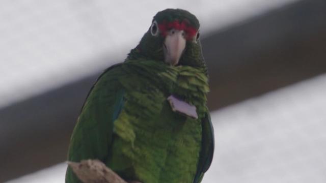
Some of the most critically endangered birds on the planet have been released back into the wild. CBS News national environmental correspondent David Schechter has more on the harsh conditions Puerto Rican parrots face, and the people working to save them.
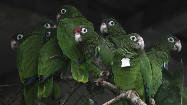
Scientists are using a range of tools to protect the endangered wildlife that could disappear in coming decades.

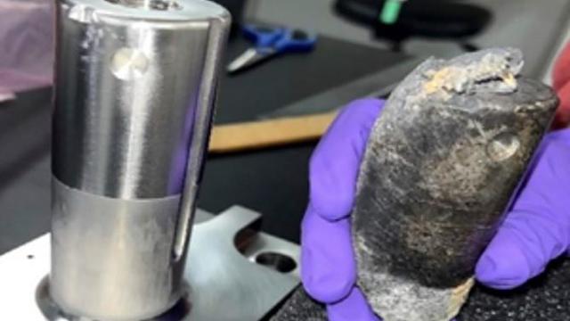
A human jawbone containing several teeth was linked to a former U.S. Marine who died almost 75 years ago during a military exercise in California.

The recent births of Noreen and Antonia are boosting hopes of diversifying the endangered species.
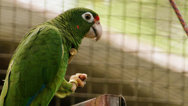
Hurricane Maria nearly wiped out an endangered parrot in Puerto Rico, highlighting the grave threat climate change-fueled storms pose to endangered species.
Prosecutors allege one of the suspects, Tifany Adams, provided a statement to law enforcement "indicating her responsibility" in the killings.
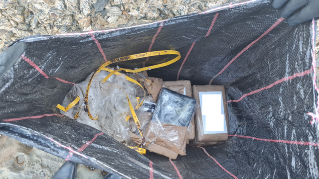
The man faces seven charges related to drug importation and dealing and 12 other charges. He faces life in prison, officials said.
Twelve people have been selected to serve as jurors in former President Donald Trump's criminal trial in New York, filling out the panel on the third day of proceedings.
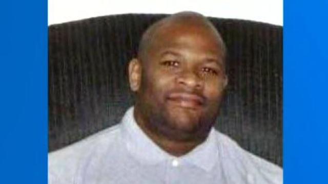
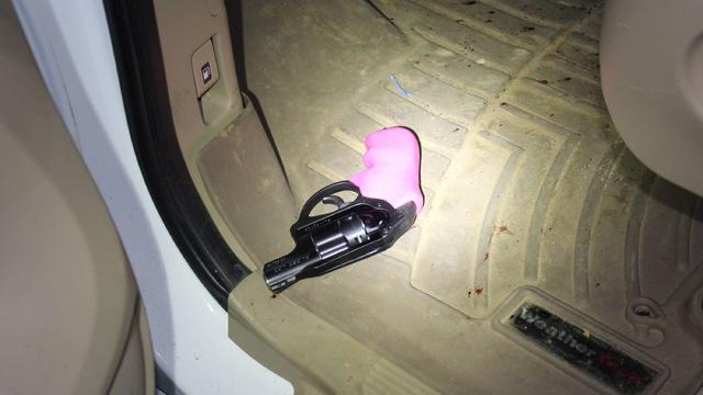
Sgt. Tony Anthony Mason Jr. was shot to death while sitting in a car with a woman he had been dating, according to police.
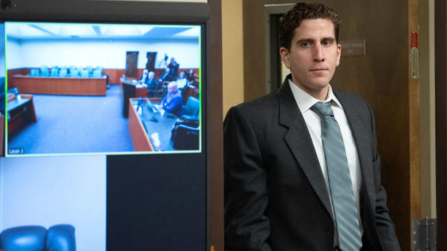
In an alibli court filing, lawyers for Bryan Kohberger, accused of fatally stabbing four University of Idaho students, claim he was "out driving" the night of the killings.
NASA confirmed Monday that a mystery object that crashed through the roof of a Naples, Florida home last month was space junk from equipment discarded by the space station.
NASA said it agrees with an independent review board that concluded the project could cost up to $11 billion without major changes.
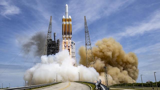
It was a "bittersweet moment" as United Launch Alliance brought the Delta program to a close.
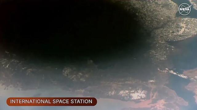
NASA flight engineers managed to photograph and videotape the moon's shadow on Earth about 260 miles below them.

Millions of Americans poured into the solar eclipse’s path of totality to watch in wonder. The excitement was shared across generations for the rare celestial event that saw watch parties across the country as almost all of the continental U.S. saw at least a partial solar eclipse.
A look back at the esteemed personalities who've left us this year, who'd touched us with their innovation, creativity and humanity.

The Francis Scott Key Bridge in Baltimore collapsed early Tuesday, March 26 after a column was struck by a container ship that reportedly lost power, sending vehicles and people into the Patapsco River.
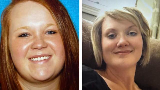
When Tiffiney Crawford was found dead inside her van, authorities believed she might have taken her own life. But could she shoot herself twice in the head with her non-dominant hand?
We look back at the life and career of the longtime host of "Sunday Morning," and "one of the most enduring and most endearing" people in broadcasting.

Cayley Mandadi's mother and stepfather go to extreme lengths to prove her death was no accident.

Two U.S. officials confirm to CBS News that an Israeli missile has hit Iran. The strike follows last weekend's retaliatory drone and missile attack against Israel. Carissa Lawson anchors a special report.
Taylor Swift's successes and failures, including the battle to regain control of her master recordings, are part of the syllabus at the University of California, Berkeley. Jo Ling Kent has more.

U.S. officials, from the president to the Treasury secretary, are accusing China of pushing cheap goods. Mark Wu, professor of law at Harvard University, joins CBS News to examine how low-priced Chinese products could impact American businesses, workers and the global economy.
Some of the most critically endangered birds on the planet have been released back into the wild. CBS News national environmental correspondent David Schechter has more on the harsh conditions Puerto Rican parrots face, and the people working to save them.
A bipartisan group of lawmakers has introduced a bill supporting the development of nuclear fusion power. Hank Jenkins-Smith, professor of public policy at the University of Oklahoma, joins CBS News to discuss.